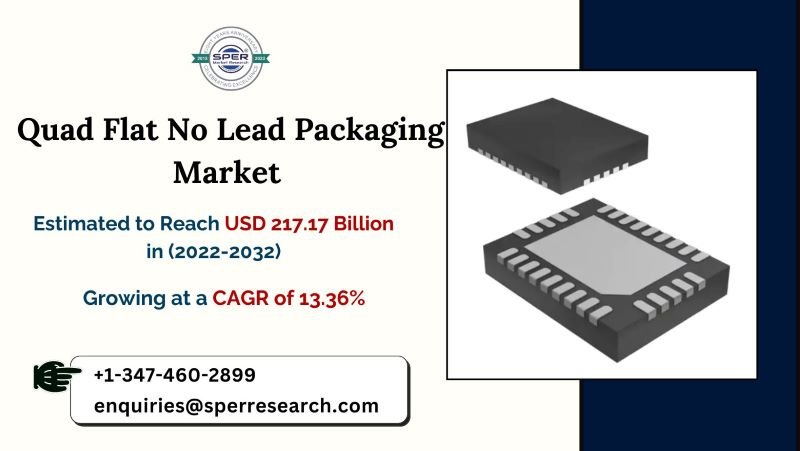
Quad Flat No-Lead (QFN) packaging is a surface-mount integrated circuit (IC) package that is widely utilized in current electronics production. QFN packages are distinguished from standard leaded packages by their flat bottom and lack of protruding leads from the sides. Electrical connections are established via pads located on the package’s bottom surface. QFN packages are available in a variety of sizes, most often square or rectangular. They are meant to be compact and space-saving, which is useful in applications where board space is limited. QFN packages are soldered directly to the surface of the printed circuit board (PCB) using solder paste and reflow soldering processes.
According to SPER Market Research, ‘Quad Flat No Lead Packaging Market Size- By Type, By Moulding Method, By Terminal Pads, By Application, By End User- Regional Outlook, Competitive Strategies and Segment Forecast to 2032’ States that the Global Quad Flat No Lead Packaging Market is estimated to reach USD 217.27 billion by 2032 with a CAGR of 13.36%.
Consumer demand for smaller and more compact gadgets has fuelled the ongoing trend of downsizing in electronics design. QFN packages have a small footprint and high integration density, making them excellent for applications that require minimal space. QFN packages provide outstanding electrical performance properties, such as reduced parasitic capacitance and inductance, which are critical for high-speed and high-frequency applications in telecommunications, computers, and automotive electronics. The architecture of QFN packages, with exposed thermal pads on the bottom surface, provides for excellent heat dispersion. As electronic devices get more powerful and compact, good thermal management becomes more critical, propelling the use of QFN packaging.
While QFN packages feature exposed thermal pads for heat dissipation, efficient thermal management can still be difficult in high-power applications or in settings with extreme temperatures. Ensuring proper heat sinking and thermal design may necessitate additional technical efforts. The long-term performance of QFN packages is dependent on the durability of solder junctions, especially under heat cycling and mechanical stress. Poor solder joint quality or insufficient solder paste deposition can cause problems like solder cracking or joint fatigue, reducing reliability. QFN packages’ small size and fine pitch make them difficult to assemble using automated production processes such as pick-and-place and reflow soldering. Accurate positioning and soldering of QFN packages necessitates sophisticated equipment and precise process control.
Request For Free Sample Report @ https://www.sperresearch.com/report-store/quad-flat-no-lead-packaging-market.aspx?sample=1
During the pandemic, many industries that relied heavily on QFN packaging, such as automotive and consumer electronics, saw lower demand. Lockdowns, economic uncertainty, and reduced consumer spending all contributed to lower manufacturing volumes and orders for electrical gadgets with QFN packaging. Many semiconductor manufacturers and assembly sites had operational issues, such as worker interruptions, social distance requirements, and interim closures. This had an influence on QFN package production capacities and capabilities, resulting in delays in order delivery and fulfillment. Research and development activities for novel QFN package designs or breakthroughs may have been delayed or temporarily suspended because to limited laboratory access, low funding, and changing focus to pandemic-related research.
QFN packaging technology is widely utilized in semiconductor manufacturing, which is mostly centered in the Asia-Pacific area. So the Asia-Pacific region dominated the worldwide market and is expected to be the fastest-growing sub-segment. Some of the Key players are Amkor Technology Inc., ASE, ChipMOS TECHNOLOGIES INC., JCET Group, Microchip Technology Inc., NXP Semiconductors, Powertech Technology Inc., STATS ChipPAC Pte Ltd,
Quad Flat No Lead Packaging Market Segmentation:
By Type: Based on the Type, Global Quad Flat No Lead Packaging Market is segmented as; Air-cavity QFN, Plastic-moulded QFN, Others.
By Moulding Method: Based on the Moulding Method, Global Quad Flat No Lead Packaging Market is segmented as; Punched, Sawn.
By Terminal Pads: Based on the Terminal Pads, Global Quad Flat No Lead Packaging Market is segmented as; Fully Exposed Terminal Ends, Pull-back Terminal Ends, Side Wettable Flank Terminal Ends.
By Application: Based on the Application, Global Quad Flat No Lead Packaging Market is segmented as; Portable Devices, Radio Frequency Devices, Wearable Devices, Others.
By End User: Based on the End User, Global Quad Flat No Lead Packaging Market is segmented as; Automotive, Communications, Computing/Networking, Consumer Electronics, Industrial.
By Region: Asia-Pacific dominated the global market in terms of geography, and it is anticipated that it will continue to develop at the quickest rate throughout the forecast period.
For More Information, refer to below link:-
Quad Flat No Lead Packaging Market Outlook
Related Reports:
Contact Us:
Sara Lopes, Business Consultant – USA
SPER Market Research
+1-347-460-2899